Chopping: a technique for noise and offset reduction
5.6. Low-power low-voltage chopped transconductance amplifier for noise and offset reduction. Chopping at high frequency.
In this section the chopping technique will be exploited in order to find a new chopper architecture capable of chopping at high frequencies [10]. Chopping is a method employed for noise and offset reduction in low frequency applications. However, there are applications where the bandwidths of signals can reach MHz range and offset and noise reduction is required. The question is if one can use the chopper technique to process signals with a large bandwidth. In this case we have to be able to increase the chopper frequency without increasing excessively the residual offset generated by second order effects. It is worth to mention that chopper architecture presented in the following sections can be used for low frequency applications also.
High-end audio applications will require dynamic ranges of more than 90dB with strong requirements on linearity. When driving headphones, excessive offset decrease the efficiency of the headphone by heating up the coil and even destroying it. In some portable audio applications, power consumption is also a matter of concern. The aim is to boost the dynamic range and the accuracy of the system without power penalty. The low-power chopped transconductance amplifier presented in the following sections is meant for portable audio applications and the principle can be used in a large variety of circuits.
5.6.1. Conventional choppers
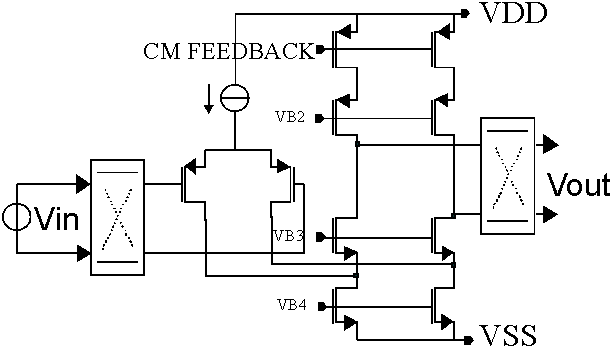
In conventional choppers [11], [12], [13] the signal is being transposed at the input of the differential pair, amplified and demodulated back at the output nodes as shown in fig.5.8. Switching at high impedance nodes [14], [15], [16] would be disadvantageous due to limited bandwidth of the amplifier. From section 5.4 was clear that we need large amplifier bandwidths in comparison to the chopping frequency. Only in this situation we have reduction of 1/f noise. A band-limited amplifier gives also second order effects like attenuation of the signal in the base-band and high frequency residues around even multiples of the chopping frequency. That is why, in this approach, high frequency chopping is not possible and this method is limited to few tens of KHz. Besides, the switching noise is directly coupled to the output. Because we have switches in the middle of the supply voltage, for low voltage applications charge pumps are needed. This is to ensure that all switches are firmly open and/or closed.
We need a low pass filter at the output to recover the base-band free of noise. For low frequency applications the required time constants for filtering cannot be integrated on-chip. Another approach would be to use a bandpass filter centered around 2fchop to recover the signal [17], [18]. In this situation, very low offsets are reported but the method is applicable for low frequencies. Besides the bandpass section would require extra power [see Chapter 3]. In reference [13] a sample and hold circuit has been used for low-pass filtering by exploiting the low-pass character of the sin(x)/x function. Again this method has been applied for low frequency applications. Theoretically, we need to chop in the signal path where there is no bandwidth limitation and if possible to eliminate the required low-pass filter.
|
|
|
Fig.5.8: Conventional choppers |
5.6.2. The proposed method
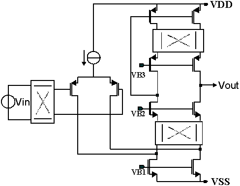
The proposed method presented in reference [10] is shown in fig.5.9. It comprises an input modulator, a PMOS differential pair, current sources and a low voltage, high bandwidth cascoded mirror, to perform a differential to single ended conversion. The second chopper transposes again the signal at low impedance nodes and demodulates back the signal, canceling out the offset of the bottom transistors. The offset and noise from the current sources will be canceled out by the third chopper which matches dynamically [19] the two transistors on top. There are no consequences on the signal due to the third chopper.
The benefit of chopping at low impedance nodes comes from the large bandwidth of the basic amplifier. Therefore, we can chop at much higher frequencies where the only limitation would be the charge injection residual offset and the slewing behavior of the input stage. In plus, the cascode transistors provide low-pass filtering for the high frequency spectral contributions coming from chopping.
In this approach charge pumps are not needed if the common mode voltage is well chosen and switching is close to the supply rails. The output node used for Miller compensation filters out the undesired high frequency spectral components from switching, delivering to the output stage an offset/noise free voltage. Another advantage is using the dominant pole of the amplifier as a low-pass filter. In the conventional approach an extra filter after the last chopper is required.
5.6.3. Circuit principle
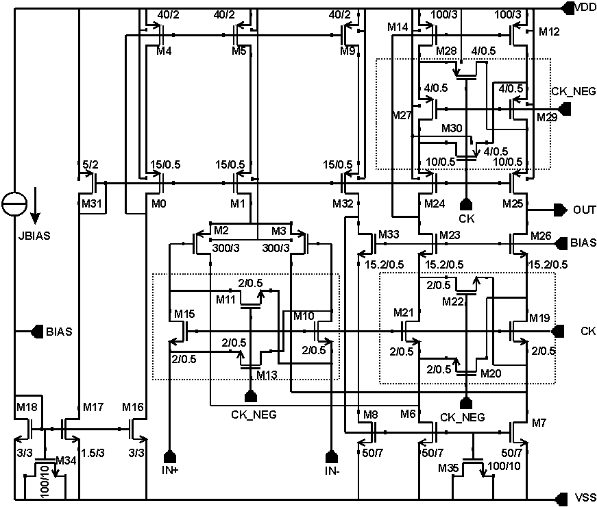
Fig.5.10 illustrates the circuit diagram. The input chopper M10, M11, M13 and M15 transposes the differential input signal applied to the terminals IN+ and IN- to the alternate output nodes. The second chopper M19, M20, M21 and M22 demodulates the signal and modulates 1/f noise and offset at odd harmonics.
|
|
Fig.5.9: The basic principle |
The cascoded mirror M24, M25, M12 and M14 performs the required broadband differential to single ended conversion at the output. The need for large bandwidths implies small transistor lengths for M12 and M14 and therefore extra offset and 1/f noise. For this reason a third chopper is being introduced in the signal path: M27, M28, M29 and M30. The transistors M12 and M14 are dynamically matched [19] without consequences on signal. The unswitched cascode transistors provide further improvement in switching noise and residual offset by low pass filtering some of the HF noise components generated from chopping and keeping low voltage swings at their sources.
Another source of concern in mixed level applications is the substrate bounce coming from the digital circuitry. Modern processes have a low ohmic substrate and that is why digital circuits pollute the substrate, generating noise in the analog circuits. In a 0.5m m CMOS technology for mixed level signal processing, the substrate bounce can reach 300mV in amplitude with spectral contributions in GHz range, further reducing the voltage swing [20]. In order to minimize substrate interferences, only PMOS transistors and NMOS switches with small dimensions are being used in the signal path [10]. The oxide capacitance of M34 decouples the BIAS line to VSS. Substrate interferences present in the sources of cascode transistors M23 and M26 will be also present at their gates such that gate source voltages of the same transistors can be considered constant for HF substrate noise [20]. For the same reason, the current sources M6 and M7 have their gates decoupled to VSS via a large capacitance [M35].
|
|
|
Fig.5.10: Circuit diagram |
5.6.4. Noise and offset
The input transistors have the largest noise contributions because they are providing the largest gain in the circuit. Noise contributions are coming from transistors M6, M7, M12 and M14. Neglecting the noise introduced by cascode transistors and switches, the power spectral density of the white and 1/f noise referred to the input is:
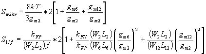
In the above equation kFN and kFP are process dependent constants. Large transconductances of the differential input pair give low white noise. 1/f noise can be minimized by increasing the area of the input pair and increasing the transconductance of the input transistors in comparison to the transconductances of M6, M7 and M12, M14. The input pair is biased in weak inversion for accuracy reasons [see Chapter 3] and white noise considerations.
Large phase margins can be obtained when M12 and M14 have small lengths. This increases their contribution to the offset and noise. The dominant terms in the offset voltage are due to threshold mismatch of the input pair and the threshold mismatch of M12 and M14. If D VT denotes the threshold mismatch, D b /b the relative gain factor mismatch, VGT the effective gate voltage (VGS-VT), n the slope factor and UT the thermal voltage, the offset voltage referred to the input can be approximated as:
 (5.20)
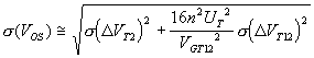
In order to reduce the influence of the threshold mismatch of M12 and M14 we have used dynamic element matching to reduce this effect. Fig.5.11 shows the simulated dynamic range (static) of the OTA and the static offset as a function of the bias current JBIAS. The 1/f noise contribution has been subtracted from the total noise. The OTA has been configured as a follower with 10MHz gain bandwidth product (GBW). By scaling down the current according to W scaling and keeping the same power supply voltage and GBW, a factor 10 reduction in power gives a 10dB reduction in DR. This can be seen also from the DR*GBW product of the OTA already discussed in Chapter 3, section 3.4.5. If PWI denotes the total power, D the saturation limits at the output node, n the slope factor, h the current efficiency and NEF the noise excess factor then:
 (5.21)
|
|
|
Fig.5.11: DR and offset as a function of bias current |
Given the efficiency h =0.16, the noise excess factor NEF=2.2 the GBW=10MHz , to reach a dynamic range of about 92dB we need a minimal power consumption of 940mW according to (5.21). From fig.5.9 the bias current for this dynamic range is 30mA and the power consumption is 590mW. From accuracy point of view by increasing the current, the offset voltage decreases. The same factor 10 increase in power consumption will generate only a factor two improvement in accuracy. This explains again that accuracy driven power gives stronger constraints than noise driven power.
5.6.5. Experimental results
The chopped transconductance amplifier has been realized in a 0.5 m m CMOS technology with two polysilicon layers and three metal layers. For measurements purposes the OTA has been configured as a follower with a bias current of 30 m A.
a. Offset measurements
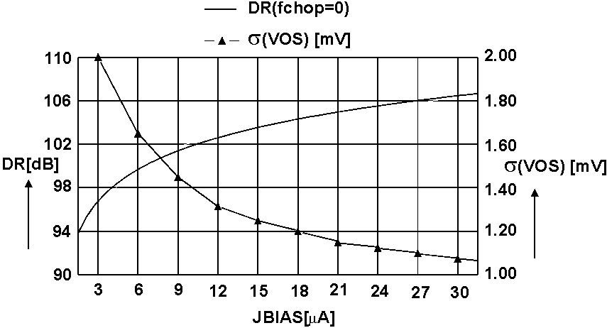
Fig.5.12 shows the static offset and the residual offset for 6 arbitrarily chosen circuit samples after low pass filtering the output. Without chopping (fchop=0), static offsets of less than Vos=680m V can occur. Chopping will reduce the offset for relatively low chopper frequencies but increasing the chopping frequency the residual offset will increase. The residual offset is generated by charge injection and mismatch between the transistors of the chopper modulator. Charge injection is a phenomenon which occurs in the switching instants due to the clock feedthrough and charge shot in the channel. At low frequencies the errors per switching period made by charge injection are negligibly small. The residual offset at 100KHz chopping frequency is less than 150m V. At high frequencies the errors generated by charge injection cannot be neglected anymore and the residual offset increases. Up to 1MHz the residual offset is lower than 370m V in all six cases. At low chopping frequencies, a minimum in the residual offset occurs. Second order effects like charge injection and residual
|
|
|
Fig.5.12: Static and residual offset |
offsets are extensively discussed in section 5.6.6.
b. Noise measurements
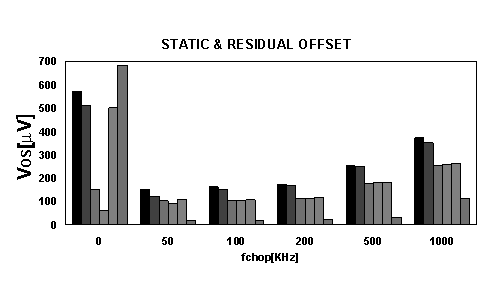
For digital audio applications there are strong requirements for linearity and signal to noise ratios. The measurements for linearity and signal to noise are merged in one measurement called SINAD, an acronym for signal to noise plus distortion. This figure is more restrictive than signal to noise because it includes also the distortion components. Fig.5.13 illustrates the signal to noise plus distortion figure (SINAD) for 93KHz chopping and 1KHz input.
|
|
|
Fig.5.13: SINAD at 93KHz chopper frequency |
The input signal at 0dB reaches 2.8Vpp where distortion is high and dominates SINAD. At this level of signals the output transistors are pulled out of saturation and the distortion is high. For low signal amplitudes the noise level is higher than the distortion level. The measured signal to noise ratio in audio band (0..20KHz) after chopping is -95dB and harmonic distortion (THD) is -89dB at -15dB signal level. Chopping increases the signal to noise plus distortion ratio with about 6dB. The power consumption is 590mW from a 3.3V power supply. The 3.3V power supply voltage comes from digital requirements. However, the OTA can work down to 1V with decreased dynamic range.
The 1/f noise decreases the dynamic range of the amplifier. The same noise performances can be achieved without chopping but increasing the power consumption 4 times (2.4mW) as estimated by eq.[5.21]. The power needed for chopping is negligible small in comparison to the bias power. In mixed level applications there is always a clock generation circuit for the digital circuits. That is why the clock circuitry for digital functions can be shared with chopped amplifiers without the need for an extra clock. At 1MHz chopping the estimated power consumption of the chopper modulators is about 10mW. In Table 5.1, a summary of performance is presented.
Special measures have been taken in order to improve matching when the layout of the circuit has been made. To reduce charge injection, the switches of the chopper modulator should be well matched. In fig.5.12 the chip photomicrograph is illustrated. The area of the OTA is about 0.03mm2. Some possible applications of the chopped transconductance amplifier include low noise and low offset applications like:
- low offset integrators for battery management where the battery current is monitored;
- high precision and low noise band-gap references in CMOS;
- headphone drivers in a D/A configuration for portable applications;
- filters where matching requires too much area and power consumption;
- sensors with high requirements on precision and temperature drifts;
|
Open-loop gain (AOL) |
>75dB |
|
GBW |
10MHz |
|
Offset(static) |
<680m V |
|
Offsetfchop<1MHz |
<370m V |
|
S/N|fchop=93KHz |
95dB |
|
S/N|fchop=0 |
89dB |
|
THD |
-89dB |
|
Supply voltage |
3.3V± 10%(min 1V) |
|
Power |
590m W |
|
Technology |
0.5m m, 2PS, 3AL, CMOS |
|
Area |
0.03mm2 |
Table 5.1: Performance summary
|
|
|
Fig.5.14: Chip photomicrograph |
5.6.6. Second order effects: Charge injection and residual offset
In the input modulator charge injection and parasitic coupling will cause spikes to appear. Although spikes are common mode signals, the common mode rejection of the amplifier is limited at high frequencies. Therefore, after amplification and demodulation, these spikes generate residual offsets. Only the odd harmonics of the chopper frequency will contribute to the residual offset. In fig.5.15 the output of the chopped OTA is shown. The OTA has been configured as a buffer which modulates its own offset. The spikes presented at the output have a time constant T0 and an amplitude Vinj. The bandwidth of the spikes is about 1/T0 larger than the chopping frequency. When the charge injection time constant T0 is small, the energy of the spikes will be located at high frequencies. If the bandwidth of the amplifier is well chosen to have sufficient gain for the modulated signal and to reject the spectral components of the spikes, the amount of residual offset generated will be reduced. The Fourier transform of the spike signal is:
![]() (5.22)
(5.22)
This spectrum is applied to the amplifier with a frequency transfer A(f). The residual offset is found from the following convolution:
 (5.23)
|
|
|
Fig.5.15: Charge injection at the output |

The first term in (5.23) represents the Fourier transform of the spikes filtered by the amplifier transfer function A(f). The second term is the Fourier representation of the chopper signal m(t). In a follower configuration, chopping is an internal operation thus, the transfer function A(f) is the gain of the input stage loaded with transistors M23 and M26. Hence, from (5.23) the residual offset can be found from the following series:
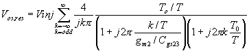
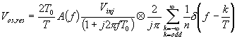
In eq.(5.24) T is the chopping period and Cgs23 the gate-source capacitance of M23 and M26. By using Poisson summation rule for series and considering gm2/2p Cgs23 larger than 1/T=fchop (condition found in section 5.4), we get:
 (5.25)
This shows an increase of the residual offset with chopping frequency and the energy of the spikes, already seen in the measurements from fig.5.12. The explanation of the large spikes in the first modulator can be found from fig.5.16. The input stage has been replaced with a capacitive load and the output stage has an output resistance R0. As long as the rise and fall times of the clock are small, the charge Dq will be equally distributed at the output of OTA and at the input stage regardless the impedance levels of the two nodes. When the output impedance of the OTA is larger than RON, the ON resistance of the switch, the dominant time constant for charge will be T0=2R0Ci and the offset will be proportional to T0 as (5.25) shows. The amplitude of the spike is Vinj=Dq/Ci. The larger the output resistance of the OTA, the larger the residual offset
|
|
|
Fig.5.16: Charge injection in the input modulator |
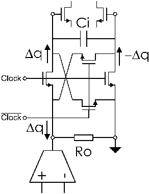
will be. In conclusion, to obtain low residual offset voltages, the output stage of the amplifier should be low ohmic. This problem will be tackled in the next chapter where an output stage will be added in order to improve residual offsets.