Chopping: a technique for noise and offset reduction
5.7. A low-power bandgap voltage reference
In the previous section an OTA for high end audio applications has been presented. The need for high dynamic range and large GBW requires few hundreds of mW of power. A bandgap reference is an example of a low frequency application where accuracy and area give constraints on the total power consumption.
In mixed level applications accurate voltage references are difficult to realize due to the lack of reproducible lateral pnp transistors and the large offsets inherent to CMOS opamps. If low power is a must, the accuracy is mainly impaired by the increased offset of the opamps. It is shown that by using chopping techniques the accuracy of a bandgap voltage reference can be improved about ten times without laser trimming and with the benefit of reducing the 1/f noise of the amplifier. This example shows that the principle of the chopped OTA meant for chopping at high frequencies, can be used also in low frequency applications.
5.7.1 The principle of the bandgap
The voltage of a bandgap reference is based on the bandgap voltage Vgap0 of a semiconductor: a well defined physical value. In submicron CMOS digital processes, the lack of reproducible lateral pnp’s can be seen as a disadvantage. Without these components one has to rely upon the well known solution for a bandgap reference shown in fig.5.17a, which requires the use of an opamp. In bipolar technologies, simple solutions for voltage references have been considered [21], [22]. For CMOS processes the large offset of the opamp will reduce the accuracy of the output voltage V0. In order to achieve better accuracy, laser trimming is a well known solution but an expensive one. At low bias currents of the opamp, the offset increases and the challenge would be the realization of a low power and accurate bandgap voltage reference in CMOS without laser trimming of resistors. Furthermore, the available area is limited. Obtaining better resistor matching by increasing the area is not an option.
When a stable reference voltage is not required at all times (as in the case of an A/D) switched-currents techniques with autozero amplifiers can provide the needed precision [23], [24]. The resulting bandgap reference voltage is not continuous time and has the disadvantage of increasing the white noise by sampling. Besides, the power consumption of the sampled data bandgap is higher than a few hundred mW.
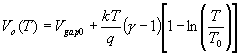
In fig.5.17b, the output voltage V0 can be related to the absolute temperature as [25]:
 (5.26)
Vgap0 denotes the extrapolated bandgap voltage of a semiconductor, g is the mobility temperature exponent of the charge carriers in a bipolar transistor and T0 the reference temperature. This condition holds true for a well chosen resistance ratio R1/R3. If n is the ratio between the emitter areas of T1 and T2, UT the thermal voltage kT/q and C1 a process constant then the ratio of resistors R1/R3 has to satisfy the following condition:
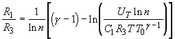 (5.27)
In fig.5.17b, a plot of eq.(5.26) centered around T0=50° C is shown. The accuracy of
|
|
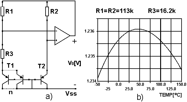
|
Fig.5.17: Basic bandgap reference |
the output voltage, at the reference temperature T0, depends on the process spread, the offset voltage of the opamp and matching of the resistors.
5.7.2 The accuracy of the bandgap
Consider the basic bandgap from fig. 5.17.a. and the deviation of the output voltage from the nominal voltage (D V0) due to the deviation of the resistances and the offset of the opamp Vos. The transistor T1 is made from n identical transistors as shown in fig.5.17a. Denote RN nominal values, R the actual values of the resistors and UT the thermal voltage. The absolute error of the reference voltage is given by:
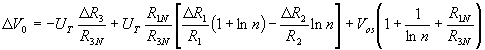
The first term is generated by the process spread of R3. The second term comes from the mismatches of the resistors R1 and R2. The last term is generated by the offset of the opamp. Now we can find the spread of the output voltage s 2(V0) as a function of the individual terms s 1...5.
![]()
where:
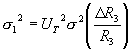
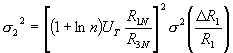
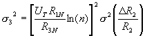
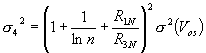
Comparing s 1...4 in (5.30) the dominant term is by far s 4. For a resistor ratio R1N/R3N of about 7 and n=24, the opamp offset voltage spread s 2(Vos) is amplified about 70 times. The simulated spread in the offset voltage of the opamp is s(Vos)=3.8mV. According to (5.30.d) this gives a spread in VO of about 32mV. Hence, in order to get a better accuracy, one should be able to decrease the offset of the opamp.
5.7.3. Accuracy improvement
In fig.5.18 we have a version of the bandgap reference based on the principle
|
|
|
Fig.5.18: Bandgap voltage reference with chopped amplifier |
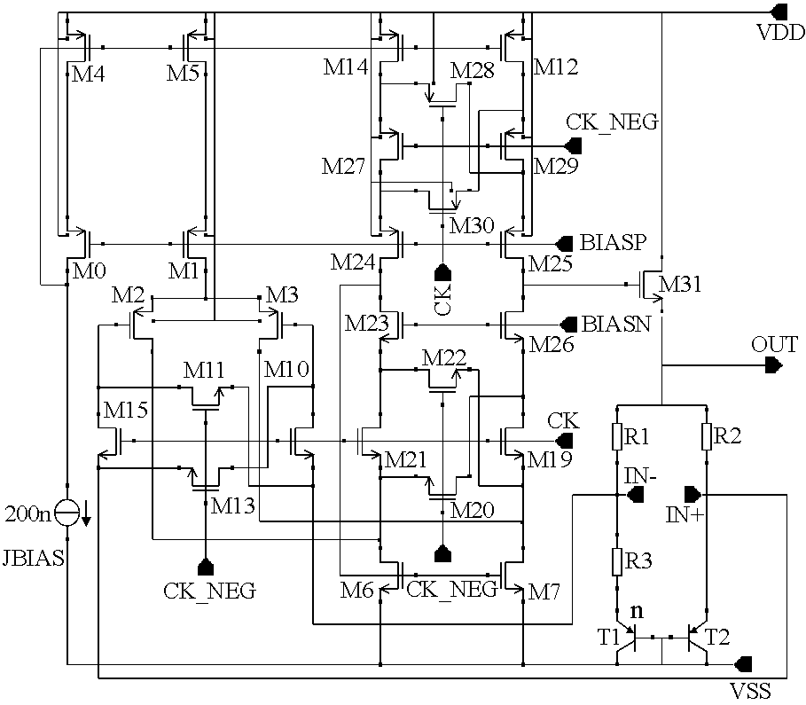
shown in fig.5.17.a with a chopped operational amplifier [26]. The source follower M31 provides the output voltage VO, bandgap referenced. Simulations shows that the spread of the opamp offset without chopping is s(Vos)=3.8mV.
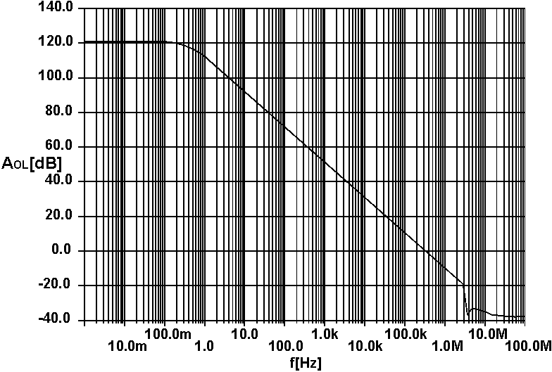
Chopping at 10KHz, the offset will be reduced to 10m V(1s ). The current consumption of the opamp is 3m A from a 2.5V power supply voltage. Fig.5.19 shows the open loop gain of the opamp. The low frequency gain is 120dB, the gain-bandwidth product of the opamp is 300kHz and the phase margin 74° . The resistors R1, R2 and R3 are polysilicon resistors with a low temperature coefficient and their values are given in fig.5.17.b. In order to decrease the spread, parallel-series configurations of equal sized resistors have been used. The area of the circuit is about 0.035mm2 being dominated by the area of the resistors.
Without chopping, the cumulated effect of the spread contributions gives 32mV(1s ) spread at the output. By chopping, the total spread reduces to 3.2mV(1s ). The accuracy of VO can be increased, in principle, by increasing the area of the resistors. Simulations show that increasing the area 16 times, the spread of the reference voltage is 1.8mV(1s ). The bias current can be derived from the bandgap referenced output in order to have a temperature independent biasing. To prevent the zero solution of the output voltage, we need to add a start-up circuit. The total power consumption of the circuit is 7.5m W.
|
|
|
Fig.5.19: The open loop gain of the opamp |
5.7.4. Noise properties:
Due to the low current levels, the transconductance of the input stage of the opamp is low and the noise properties of the bandgap are dominated by the opamp white noise. The 1/f noise is being reduced by the chopping mechanism and therefore the power spectral density of the noise at the output depends on the noise properties of the opamp. Denote NEF the noise excess factor of the opamp and rD the incremental resistance of the diode connected transistor T1. The power spectral density of the output noise can be approximated with:
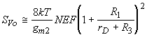 (5.31)
The closed loop bandwidth is 30kHz and the rms value of the integrated voltage noise in this frequency band has a value of about 67m Vrms for an opamp noise excess factor NEF of 2.2.